


Revolutionizing Semiconductor Production: University of Southampton Introduces Cutting-Edge E-Beam Lithography Facility
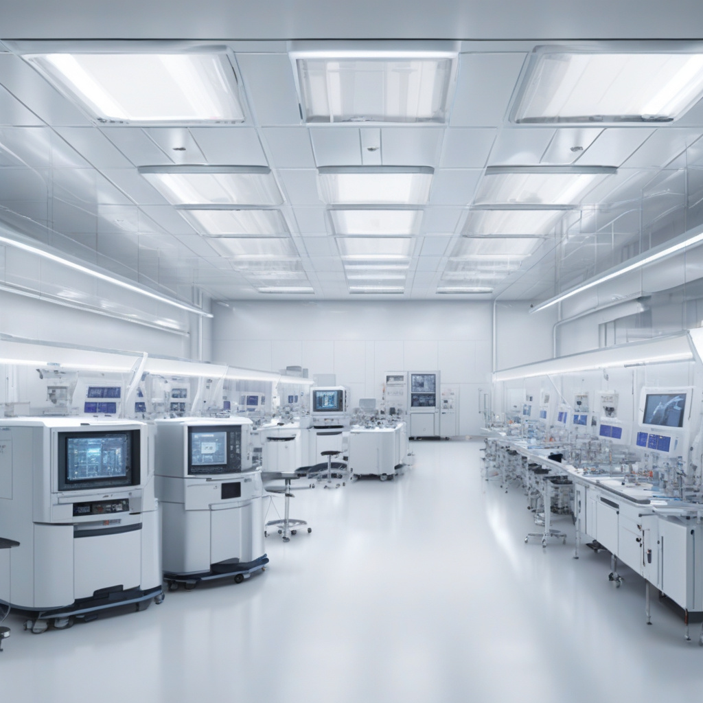
In a groundbreaking move that is set to redefine the landscape of semiconductor manufacturing, the University of Southampton has unveiled a state-of-the-art facility dedicated to harnessing the power of E-beam lithography. This cutting-edge technology represents a significant leap forward in the production of semiconductor chips, paving the way for the development of the next generation of high-performance electronic devices.
The new facility, which is equipped with cutting-edge E-beam lithography tools, is poised to revolutionize the way semiconductor chips are produced. Unlike traditional photolithography techniques, which use light to pattern semiconductor wafers, E-beam lithography leverages a focused beam of electrons to achieve unparalleled precision at the nanoscale level. This level of precision is crucial for the development of advanced semiconductor devices with smaller feature sizes and higher processing speeds.
One of the key advantages of E-beam lithography is its ability to overcome the limitations of traditional lithography techniques, which are reaching their physical limits in terms of miniaturization. By using a focused electron beam to directly write patterns on the semiconductor substrate, researchers can achieve feature sizes that were previously thought to be unattainable. This breakthrough technology opens up new possibilities for the design and manufacture of cutting-edge electronic devices, including high-performance processors, memory chips, and sensors.
The University of Southampton’s investment in E-beam lithography underscores its commitment to fostering innovation and driving technological advancements in the field of semiconductor research. By providing researchers and industry partners with access to state-of-the-art lithography tools, the university is creating a collaborative environment where groundbreaking ideas can be transformed into reality.
The implications of this new facility extend far beyond the confines of the university campus. The development of next-generation semiconductor chips has the potential to revolutionize a wide range of industries, from telecommunications and computing to healthcare and automotive. These advanced chips will power the devices of the future, enabling faster data processing, lower power consumption, and enhanced functionality across the board.
Moreover, the University of Southampton’s E-beam lithography facility is poised to play a pivotal role in driving economic growth and technological innovation in the region. By attracting top talent and fostering collaborations with industry partners, the university is positioning itself as a hub for cutting-edge research and development in the semiconductor industry.
As we stand on the cusp of a new era in semiconductor technology, the University of Southampton’s investment in E-beam lithography represents a significant milestone in the journey towards innovation and progress. By pushing the boundaries of what is possible in semiconductor manufacturing, researchers at the university are laying the foundation for a future where electronic devices are faster, more powerful, and more energy-efficient than ever before.
In conclusion, the introduction of the E-beam lithography facility at the University of Southampton marks a significant step forward in the production of the next generation of semiconductor chips. By leveraging the power of electron beams to achieve unparalleled precision and miniaturization, researchers are opening up new possibilities for the design and manufacture of high-performance electronic devices. As we look towards the future, it is clear that this cutting-edge technology will play a central role in shaping the technological landscape for years to come.
semiconductor, lithography, innovation, technology, University of Southampton