


EU Approves €1.3bn Funding for Semiconductor Advanced Packaging Facility
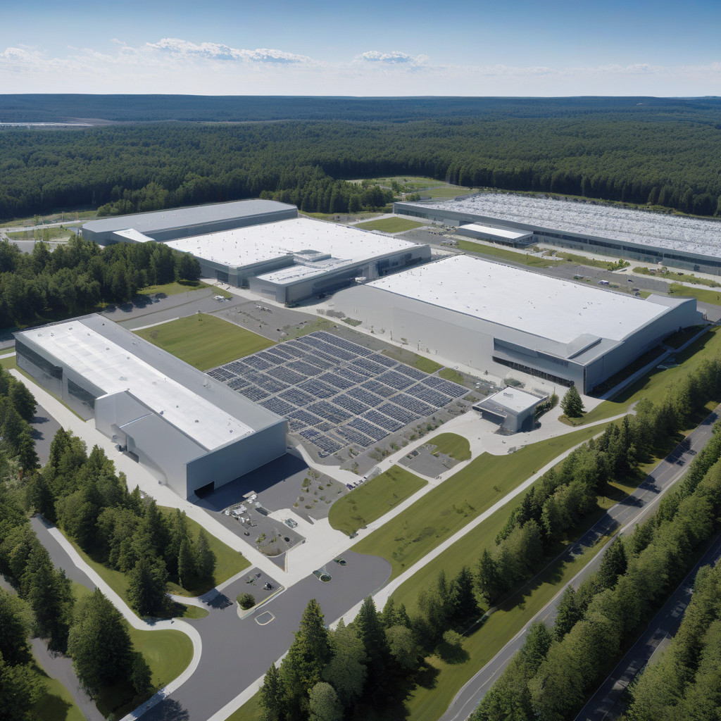
The European Union Commission has taken a significant step forward in bolstering the semiconductor industry by approving €1.3 billion in funding to support the establishment of a cutting-edge semiconductor advanced packaging facility in Novara, Italy.
Semiconductors are the backbone of modern technology, powering everything from smartphones and computers to cars and medical devices. However, the global semiconductor shortage highlighted the urgent need to ramp up production capacity and reduce reliance on a few key players in the market. The EU’s decision to invest heavily in a semiconductor advanced packaging facility demonstrates a commitment to strengthening Europe’s semiconductor industry and securing the region’s technological sovereignty.
The facility in Novara, Italy, will play a crucial role in advancing semiconductor packaging technology, which is essential for enhancing the performance, power efficiency, and reliability of semiconductors. By focusing on advanced packaging, the facility will enable the integration of multiple functions into a single chip, paving the way for smaller, faster, and more energy-efficient devices.
This investment aligns with the EU’s strategic goals of fostering innovation, boosting competitiveness, and creating a more resilient and sustainable economy. The semiconductor advanced packaging facility is expected to drive technological advancements, create high-skilled jobs, and contribute to the growth of the semiconductor ecosystem in Europe.
Furthermore, the establishment of the facility in Novara will strengthen Europe’s position in the global semiconductor market and reduce its dependence on imports from other regions. By building a state-of-the-art semiconductor packaging facility on European soil, the EU aims to enhance its technological independence and ensure a stable supply of critical components for key industries.
The funding approval signals a significant milestone in Europe’s efforts to build a robust semiconductor industry that can compete on a global scale. It underscores the EU’s recognition of the strategic importance of semiconductors in driving innovation, digital transformation, and economic growth.
As the demand for semiconductors continues to rise across various sectors, including automotive, healthcare, telecommunications, and renewable energy, investing in advanced packaging technology is crucial for meeting the evolving needs of the market. The semiconductor advanced packaging facility in Novara will serve as a catalyst for innovation and enable European companies to develop cutting-edge semiconductor solutions that address current and future challenges.
In conclusion, the EU’s decision to allocate €1.3 billion in funding for a semiconductor advanced packaging facility in Novara, Italy, underscores the importance of semiconductor technology in driving Europe’s digital transformation and economic development. By investing in advanced packaging capabilities, Europe is positioning itself as a key player in the global semiconductor market and paving the way for a more competitive and innovative future.
#EUCommission, #SemiconductorIndustry, #AdvancedPackagingFacility, #TechnologicalSovereignty, #EuropeanEconomy